semiconductor bonding technology How to lay the solid foundation for semiconductor fabrication in india

If you are searching about Wire Bonding Technology & Surface Finished Wire Bonding Pcb you’ve came to the right place. We have 9 Images about Wire Bonding Technology & Surface Finished Wire Bonding Pcb like Wire Bonding Technology & Surface Finished Wire Bonding Pcb, Pin on The Mega Guide and also How To Lay The Solid Foundation For Semiconductor Fabrication In India. Here it is:
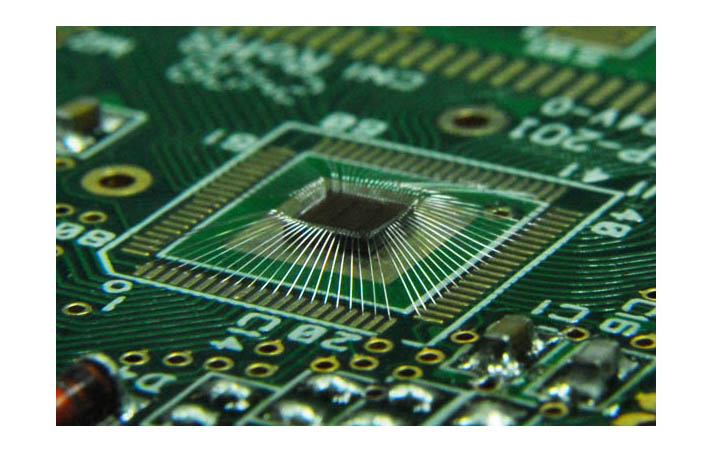
Wire Bonding Technology & Surface Finished Wire Bonding Pcb
www.rocket-pcb.com
bonding semiconductor enepig plating
Wide Bandgap Semiconductors Will Transform Electronic Products | 2014

www.assemblymag.com
semiconductors wide bandgap electronic transform faster efficient smaller silicon allows components courtesy technology than made
Semiconductor – Micro-Mechanics

www.micro-mechanics.com
semiconductor bonding mechanics
9780471574811: Semiconductor Wafer Bonding: Science And Technology: 33

www.zvab.com
Tiny Defects In Semiconductors Created ‘speed Bumps’ For Electrons

newsroom.ucla.edu
semiconductor defects ucla bumps semiconductors tiny speed electrons researchers manufacturing rendering assembly cleared path created
Pin On The Mega Guide

www.pinterest.com
semiconductor bonding covalent
Wire Bonding – HCS
www.hesse-customersolutions.com
bonding semiconductor hesse aerospace
How To Lay The Solid Foundation For Semiconductor Fabrication In India

www.forbesindia.com
semiconductor
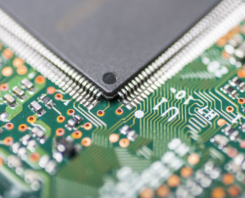
Types Of Wire Bonding – Printed Circuit Board Manufacturing & PCB

www.raypcb.com
bonding
Bonding semiconductor enepig plating. Types of wire bonding. 9780471574811: semiconductor wafer bonding: science and technology: 33
if you are looking this site you are coming to the right page. Contains many images about. Don’t forget to bookmark this page for future reference or share to facebook / twitter if you like this page.


